- 您现在的位置:买卖IC网 > Sheet目录337 > LT3492IFE#TRPBF (Linear Technology)IC LED DVR HP CONST CURR 28TSSOP
LT3492
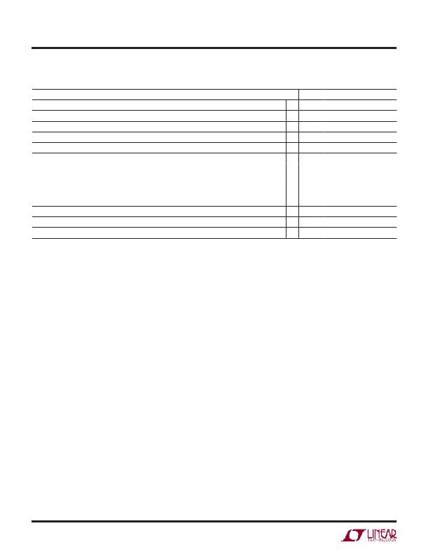
ELECTRICAL CHARACTERISTICS The l denotes the speci?cations which apply over the full operating
temperature range, otherwise speci?cations are at T A = 25°C. V IN = 5V, SHDN = 5V, PWM1-3 = 5V, FADJ = 0.5V, CTRL1-3 = 1.5V,
OVP1-3 = 0V, unless otherwise noted.
PARAMETER
CONDITIONS
MIN
TYP
MAX
UNITS
ISP1-3 Input Bias Current
ISP1-3, ISN1-3 Idle Input Bias Current
ISP1-3, ISN1-3 Input Bias Current in Shutdown
PWM1-3 = 0V
SHDN = 0V
180
250
1
1
μA
μA
μA
SHDN Input Low Voltage
SHDN Input High Voltage
1.5
0.4
V
V
SHDN Pin Current
SHDN = 5V, Current Into Pin
65
120
μA
PWM1-3 Input Low Voltage
PWM1-3 Input High Voltage
1.2
0.4
V
V
PWM1-3 Pin Current
Gate Off Voltage (ISP1-3–TG1-3)
Current Into Pin
ISP1-3 = 60V, PWM1-3 = 0V
160
0.1
210
0.3
μA
V
Gate On Voltage (ISP1-3–TG1-3)
Gate Turn-On Delay
Gate Turn-Off Delay
ISP1-3 = 60V
C LOAD = 300pF, ISP1-3 = 60V (Note 5)
C LOAD = 300pF, ISP1-3 = 60V (Note 5)
5.5
6.5
110
110
7.5
V
ns
ns
Note 1: Stresses beyond those listed under Absolute Maximum Ratings
may cause permanent damage to the device. Exposure to any Absolute
Maximum Rating condition for extended periods may affect device
reliability and lifetime.
Note 2: The LT3492E is guaranteed to meet performance speci?cations
from 0°C to 125°C junction temperature. Speci?cations over the –40°C
Note 3: Current ?ows into pin. Current limit and switch V CESAT is
guaranteed by design and/or correlation to static test.
Note 4: Absolute maximum voltage at the V IN and SHDN pins is 40V for
nonrepetitive 1 second transients, and 30V for continuous operation.
Note 5: Gate turn-on/turn-off delay is measured from 50% level of PWM
voltage to 90% level of gate on/off voltage.
to 125°C operating junction temperature range are assured by design,
characterization and correlation with statistical process controls. The
LT3492I is guaranteed over the full –40°C to 125°C operating junction
temperature range.
3492fa
4
发布紧急采购,3分钟左右您将得到回复。
相关PDF资料
LT3496IUFD#PBF
IC LED DRVR WHT/RGB BCKLT 28-QFN
LT3497EDDB#TRMPBF
IC LED DRIVR WHITE BCKLGT 10-DFN
LT3498EDDB#TRPBF
IC LED DRVR WT/OLED BCKLGT 12DFN
LT3517HUF#PBF
IC LED DRIVER AUTOMOTIVE 16-QFN
LT3519EMS-2#PBF
IC LED DRVR HP CONST CURR 16MSOP
LT3590ESC8#TRMPBF
IC LED DRVR WHITE BCKLGT SC-70-8
LT3591EDDB#TRMPBF
IC LED DRIVER WHITE BCKLGT 8-DFN
LT3593ES6#TRMPBF
IC LED DRIVR WHITE BCKLGT TSOT-6
相关代理商/技术参数
LT3492IFEPBF
制造商:LINER 制造商全称:Linear Technology 功能描述:Triple Output LED Driver with 3000:1 PWM Dimming
LT3492IFETRPBF
制造商:LINER 制造商全称:Linear Technology 功能描述:Triple Output LED Driver with 3000:1 PWM Dimming
LT3492IUFD
制造商:LINER 制造商全称:Linear Technology 功能描述:Triple Output LED Driver with 3000:1 PWM Dimming
LT3492IUFD#PBF
功能描述:IC LED DRIVER TRIPLE 28QFN RoHS:是 类别:集成电路 (IC) >> PMIC - LED 驱动器 系列:- 标准包装:6,000 系列:- 恒定电流:- 恒定电压:- 拓扑:开路漏极,PWM 输出数:4 内部驱动器:是 类型 - 主要:LED 闪烁器 类型 - 次要:- 频率:400kHz 电源电压:2.3 V ~ 5.5 V 输出电压:- 安装类型:表面贴装 封装/外壳:8-VFDFN 裸露焊盘 供应商设备封装:8-HVSON 包装:带卷 (TR) 工作温度:-40°C ~ 85°C 其它名称:935286881118PCA9553TK/02-TPCA9553TK/02-T-ND
LT3492IUFD#TRPBF
功能描述:IC LED DVR TRPL PWM DIM 28TSSOP RoHS:是 类别:集成电路 (IC) >> PMIC - LED 驱动器 系列:- 标准包装:6,000 系列:- 恒定电流:- 恒定电压:- 拓扑:开路漏极,PWM 输出数:4 内部驱动器:是 类型 - 主要:LED 闪烁器 类型 - 次要:- 频率:400kHz 电源电压:2.3 V ~ 5.5 V 输出电压:- 安装类型:表面贴装 封装/外壳:8-VFDFN 裸露焊盘 供应商设备封装:8-HVSON 包装:带卷 (TR) 工作温度:-40°C ~ 85°C 其它名称:935286881118PCA9553TK/02-TPCA9553TK/02-T-ND
LT3492IUFDPBF
制造商:LINER 制造商全称:Linear Technology 功能描述:Triple Output LED Driver with 3000:1 PWM Dimming
LT3492IUFDTRPBF
制造商:LINER 制造商全称:Linear Technology 功能描述:Triple Output LED Driver with 3000:1 PWM Dimming
LT3493
制造商:LINER 制造商全称:Linear Technology 功能描述:1.2A, 750kHz Step-Down Switching Regulator in 2mm × 3mm DFN
